The press releases on this website are provided for historical reference purposes only.
Please note that certain information may have changed since the date of release.
August 30, 2000
Sony Corporation today announced plans to establish a new semiconductor plant in Kumamoto Prefecture, Japan. The new plant will expand the manufacturing capacity of small-size LCD (high temperature Poly-Silicon) and CCD image sensors that are currently being produced at Sony Kokubu Corporation. Construction for the new plant will begin in November 2000, and production is due to start in October 2001.
In light of the strong demand for small-size LCD and CCD image sensors, Sony has decided to further strengthen its competitiveness in this market by establishing a new mass production facility. Small-size LCDs are key devices for data projectors, rear projection televisions and Camcorders, whereas CCD image sensors are critical components for digital still cameras and Camcorders.
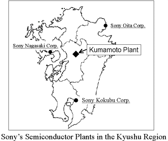
Kumamoto-prefecture is located in the center of Kyushu Island where 30% of Japanese semiconductors are produced. Not only does Kumamoto have abundant human/natural resources and semiconductor infrastructure, its proximity to Sony's other semiconductor facilities such as Sony Kokubu Corporation, Sony Nagasaki Corporation and Sony Oita Corporation facilitates the sharing of technology and raw materials.
The new plant will be the first Sony plant to comply with the production of 300mm wafers, and will also house the latest semiconductor manufacturing technologies such as localized cleanroom technology, mini production line and "zero-emission" recycling process of cleansing fluids. Initial capital expenditure is estimated at 10 billion yen within the fiscal year 2000, and cumulative investment is forecasted at 100 billion yen by the end of fiscal year 2005. The plant will employ approximately 300 people at start up, of which 140 will be new hires. Mass production of LCDs is planned to begin in 2002 at 3,000 wafers per month, and CCDs in 2003 at 2,000 wafers per month. Within 2005, production will be increased to 12,000 wafers per month, which will double the current monthly production of LCDs and CCDs (850,000 units and 2,600,000 units respectively).
| Beginning of Construction | November 2000 |
| Activation Date | October 2001 |
| Address | Kumamoto Second Techno Park Kikuchi-gun, Kumamoto Prefecture |
| Production Facility | Consecutive production from wafer fabrication to final assembly |
| Manufactured goods | High-temperature Poly-Silicon LCDs, CCDs |
| Site Area | 149,409m2 |
| Cleanroom area | 20,000 m2 |
| Clearnroom level | Class 1,000 (0.1microns) |
| Production Capacity | 2002- 3,000 wafers at start up 2005- 12,000 wafers |
| Number of Employees | Approx. 300 people at start up |
