The press releases on this website are provided for historical reference purposes only.
Please note that certain information may have changed since the date of release.
February 8, 2010

Realizes 11Gbps transfer speed with an active footprint of just 0.13mm2
Tokyo, Japan, February 8, 2010 - Sony Corporation ('Sony') today announced the development of millimeter-wave wireless intra-connection technology that realizes high speed wireless data transfer inside electronic products such as television sets. By replacing complicated wires and internal circuitry with wireless connections, this technology enables a reduction in the size and cost of the IC and other components used in electronics products, delivering advantages such as size and cost-reduction and enhanced reliability of the final product.
The advancing functionality of today's electronics products requires ever increasing quantities of internal data transfer. Once wired connections approach the limit of their data capacity, additional circuitry is required to facilitate larger data transfers, however this leads to the issue of increasingly complicated IC packages, intricately printed circuit boards, and larger IC sizes.
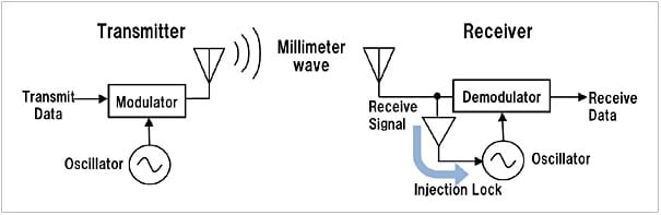
This new wireless intra-connection system is based on millimeter-wave wireless data transfer technology. Millimeter-wave refers to electromagnetic waves with a frequency of 30GHz to 300GHz, and wavelength between 1mm to 10mm. With their high frequency, millimeter-waves are suited to ultra high speed data transfer, while a further advantage is their ability to transfer data using only very small antennas. The high frequency technologies used in this system also draw on Sony's extensive expertise and years of experience in the field of wireless communications and broadcast products. Specifically, Sony has integrated highly energy efficient millimeter-wave circuits on 40nm-CMOS-LSIs (with an active footprint of just 0.13mm2 including both the transmitter and receiver), to realize high speed, 11Gbps data transfer over a distance of 14mm using antennas approximately 1mm in size.
By replacing physical circuitry in electronics products with high speed wireless connections, this new data transfer technology reduces the number of wired connections and minimizes IC use, to simplify the IC package and printed circuit board. Furthermore, because the data transfer occurs without contact, this enhances the reliability of movable and detachable parts within the product.
Sony will proceed with efforts to adopt this technology in a range of electronics products, while continuing its development to meet ever-increasing data-rate requirements.
This technology will be presented at "ISSCC 2010", to be held in San Francisco, California, US, from February 7th 2010.
This technology, used together with miniature antennas approximately 1mm in length, enable transmission speeds of 11Gbps over a distance of 14mm, with power consumption of 70mW. It is possible for this distance to be extended to around 50mm using high directivity antennas.
Millimeter-Wave Intra-Connection Solution