
Chapter 5
Image Sensor Development
Part 1 CCD Development Woes
Sat within Sony Research Center in 1970, Shigeyuki Ochi furiously reads a journal article shared with him by a colleague. The paper gripped in his hands describes the invention of the CCD (charge-coupled device) by American researchers at Bell Labs earlier in April of that year. His eyes quickly darting around the page as he analyzes the CCD's structure, he soon noticed its stark resemblance to his own research subject, MOS (metal-oxide-semiconductor) components. "Although the structure itself is simple, it's a supremely interesting device," he thought. "If developed further, it could become a versatile device used for a wide range of purposes." Ochi soon began researching both CCDs and MOS devices.
Through his experiments, Ochi discovered that by using a CCD as a photosensor and converting the absorbed light into an electrical signal, the signal could then be read by another device to reconstruct the image. Starting with a rudimentary eight pixels, he eventually succeeded in reproducing a sixty-four-bit image of the letter S using a CCD. Ochi's mind raced: by installing one such device behind a camera lens, the CCD could become a sort of "digital eye." If this concept was developed further, it could lead to the mass production of low-cost lightweight cameras with exceptionally stable image quality. A future where people the world over could enjoy new forms of photos and images using Sony's cameras came rushing into Ochi's mind. Yet even Bell Labs, the technology's inventor, had already given up on further CCD development; other companies were also beginning to throw in the towel on CCD research by 1972.
Upon learning of Ochi's work on CCDs, then-Sony Vice President and head of the Sony Research Center Kazuo Iwama knew that they had to make a product using the new technology, soon officially ordering research on CCD development to fully begin. Having seen CCDs for himself while stationed in the United States, Iwama saw this as a chance for Sony to reclaim its position as a world-class semiconductor manufacturer and developer - especially after Sony had lost that status when it withdrew from developing MOS transistors for calculators, despite once being one of the world's top transistor developers.
Iwama immediately surmised that their main competitors would be American photo and film company Eastman Kodak. Ochi and the others were initially doubtful that a company in such an unrelated sector to Sony would become their competitor, until Iwama made his goal clear: to develop a high-quality and lightweight CCD camera costing under fifty thousand yen in five years or less. Iwama was fully aware that CCD cameras and VTRs could potentially create an entirely new market, one competing directly with the highly successful and established photo-film industry, and so he deliberately proposed the harsh roadmap and prospect of competing with Kodak in order to light a fire under Ochi and his team. Thus, in November 1973, all the researchers and their projects were moved from the factory to the Research Center. They were to fully focus on developing the CCD "digital eye."
While development naturally focused on the basic functionalities of image sensitivity and resolution, there was also the need to deal with issues regarding imaging defects, including spots caused by dust particles and white streaks caused by heavy metal contamination. As research difficulties mounted, more and more companies were withdrawing from CCD research by the day, returning to researching MOS-type imaging components. Sony, however, did not have such back-up projects to return to.
It was this pressure of needing to develop everything from scratch while their backs were against the wall that became the team's source of motivation.
Unfortunately, semiconductor research was not cheap. The prospect of canceling the research outright was proposed multiple times, and Iwama had to counteract the pressure Ochi's team was feeling from inside the company with his own encouragement and watchful eye. Iwama's support was indeed invaluable, as the researchers often received inspiration through a quiet remark Iwama would make here or there. Iwama's dislike of vague qualitative answers also taught his team to make records accurately and quantitatively in their reports.
Iwama was not immune to the pressure himself, however, as CCD research took a great deal of courage and perseverance on his part as well. The project required a vast amount of both monetary investment and time, and would have been thoroughly impossible had they simply been looking to turn a quick and immediate profit. When speaking to Ohga, who was in charge of approving the project's budget, Iwama had in fact said countless times, "I honestly don't know if we can make back what we've invested on CCD research even by the end of the century." Though perhaps revealing some of Iwama's worries about the project, he was clearly resolved to see it through to the end, no matter how long it took.
With Iwama backing them up, Ochi's team worked furiously at steadily increasing their CCD's pixel count, finally achieving 120,000 pixels in 1978. Seeing the clear and flawless picture after overcoming all the hurdles thus far, Iwama reportedly muttered, "we've finally done it," under his breath.
Once mass producing CCDs started becoming a possibility in 1982, however, Iwama's health began to fail him. By the time CCDs began mass production and commercial camera-style VTRs (the earliest camcorders) landed on the market, the man who should have been celebrating most joyfully had already tragically passed away. His successor, Ohga, who had risen to the position of company president, took one of the CCD chips from the very first mass production lot and brought it to Iwama's grave.
"Iwama-san, we've finally started producing the CCDs you spent all those years on," he said, as he affixed the CCD to the back of Iwama's headstone. That same CCD, withstanding rain and shine, continued to welcome the people gathering to pay their respects on each anniversary of Iwama's passing for six long years.

The Letter "S" from a 64 Pixel CCD Image Sensor (1972)

Iwama at the Atsugi Factory, Semiconductor Group (1980)

Iwama at the Sony Research Center (1981)
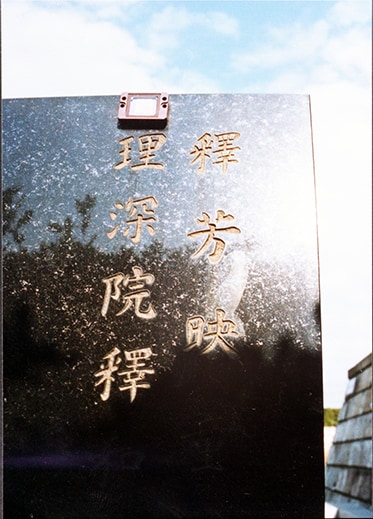
The CCD Chip Affixed to Iwama's Grave
Part 2 The Path to CCD Mass Production

CCD Production Line at Sony Kokubu
Though Iwama's wish would ultimately come to pass, it would be a harsh journey to finally begin mass producing CCDs.
Rewinding slightly to 1978, as the project transitioned from development to production, the main stage in turn shifted away from the Research Center to the Atsugi Factory. Experimental production of the 120,000-pixel CCD had begun, eventually becoming the commercially available ICX008 chip the next year. Development up until this point had cost a staggering twenty billion yen. In November of the same year, an assembly line for a prototype CCD color camera was finally completed.
It was in January 1980 when at last, the XC-1, the world's first CCD color camera featuring the ICX008 CCD image sensor, was completed and chosen to be used in thirteen of All Nippon Airways' jumbo jets for its "SKY VISION" display, providing passengers a view of both takeoff and landing. At this point, however, CCD yield rates were abysmal, with a single successful unit being produced only after several hundred failures, to the extent that people working on the project were remarking that "by definition this isn't a `yield rate,' it's a `detection rate.'" Producing the fifty-two CCD chips needed for the thirteen jets took an entire year and cost far more than the project was allowed.
The biggest issue was micron-sized dust particles invisible to the human eye. All zones related to CCD development and production were fitted with cleanrooms and suits to eliminate as much dust as possible from the environment. Whether it be human or machine, any and all sources of dust were dealt with thoroughly and with extreme prejudice.
Yield rates finally started to improve after all this effort, and CCD mass production began in 1983 at Sony Kokubu Semiconductors (current day Sony Semiconductor Manufacturing) in Kagoshima Prefecture. The war on dust was far from over, however. Though plans had ostensibly been drawn to eliminate dust from the manufacturing environment, machines, materials, and the manufacturing process itself, dust sources had not been completely eliminated from the Kokubu assembly line even after bringing the CCD-V8 video camera to market in 1985. It was for this reason that sales of a new 8mm video camera model had to be put on hold - which in the highly competitive 8mm market could spell a death sentence for a new product, and which led to severe blowback from distributors.
It was all too clear that the dust problem had to be eliminated once and for all. All the employees at the factory began tracking down dust sources and eliminating them one by one, and only by completing this monumental task, taking the hard efforts of countless employees, did yield rates finally begin to recover.
Only after this series of hardships did CCDs become a major component of Sony's success in semiconductor manufacturing. CCDs further shrank in size and grew in pixel count throughout the 80s, going from two-thirds inch chips to half-inch chips, and from 250,000 pixels to 380,000 pixels. One-third inch chips were developed in the 90s, as well as a one-inch two-million-pixel chip used for high-definition imaging. Production capacity was also expanded as mass production techniques were improved, with another factory joining Sony Kokubu in Kyushu, established as Sony Nagasaki in 1989.
CCD demand from other companies also began to grow, especially with the proliferation of consumer camcorders beginning in 1988, and Sony celebrated its ten millionth manufactured CCD in May 1990. Though this was eleven years since Sony first started CCD production, it was only 1.5 years since the five millionth CCD was manufactured, showcasing Sony's successful expansion of its production capabilities. The realm of possibility for CCDs would only continue to grow over the years, from digital cameras to computers, medicine, security, robots, and more.